

VTech PCB’s PCB development team is ready to work with circuit and application experts to bring your design to life. Working side by side with your layout team, VTech PCB provides real-time input to reduce development schedules and ensure designs are completed to specifications. Your engineers are welcome to work with us at VTech PCB, or we can deploy our layout experts to your site.
VTech PCB’s PCB layout experts can create designs for high-complexity, high-speed, and high-layer-count boards. Our symbol and footprint services are available as standalone services or as part of a comprehensive PCB layout solution.
Our layout team stays up to date with the latest technologies and successfully integrates modern PCB design practices. Some of the technologies we implement include:
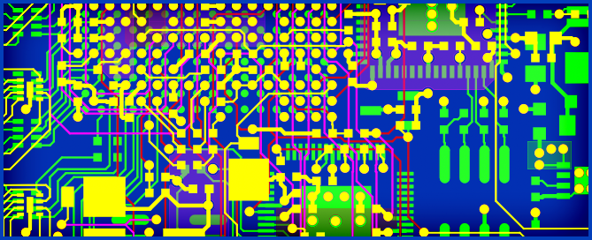
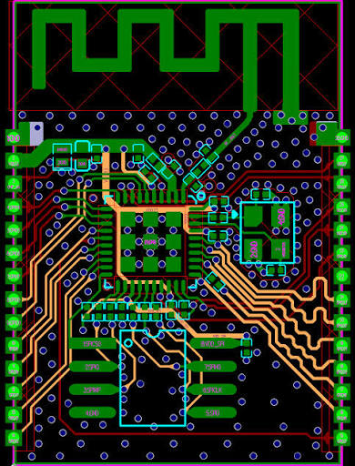
Our hardware and PCB design teams use a range of schematic capture and PCB layout tools to develop and implement printed circuit board designs that meet project specifications and performance requirements.
Cadence and Altium
Cadence and Altium
Cadence and Altium
Signal integrity is a critical aspect of high-speed PCB design, helping ensure that signals meet performance expectations and design requirements.
As signal speeds continue to increase, relying solely on general PCB routing guidelines is often insufficient. Signal integrity analysis helps identify potential issues before prototype fabrication and laboratory testing, improving signal quality, reliability, and overall design performance.
VTech PCB’s experienced design team can utilize specialized software tools for signal integrity analysis based on each customer’s specific project requirements.
Cadence SPECTRAQuest
Copyright @2026, VTECH PCB. All Rights Reserved