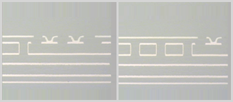
The Build-Up Board is a high-precision method used in PCB manufacturing, where multiple layers are stacked together and patterned simultaneously. This technique involves piling layers of material to form a multi-layer PCB, with each layer contributing to the overall structure and functionality.
Additionally, micro holes are created in the inner layers as needed to enable electrical conductivity between layers. The Build-Up Method is particularly effective for high-density interconnects (HDI), allowing for compact, complex designs while maintaining performance and reliability. This process is widely used in advanced electronics, where space efficiency and signal integrity are critical.
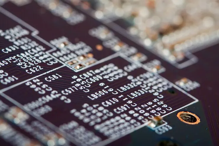
Prototype Board
The Prototype Board is designed for the initial development and testing of PCB designs, offering flexibility in surface finishing and solder mask color options. It can be manufactured with various surface finishes such as HASL (Hot Air Solder Leveling), ENIG (Electroless Nickel Immersion Gold), or OSP (Organic Solderability Preservative) to meet specific performance and durability requirements.
Structure
Ready to discuss your
PCB project?
Contact us today to learn more about our capabilities and how we can help you bring your ideas to reality.